CXMT Puts an 11.95-Nanometre DRAM Platform Into Production
The Hefei chipmaker says its fifth-generation platform yields at least 50% more dies per wafer than its fourth. It has not said how many of those dies work.
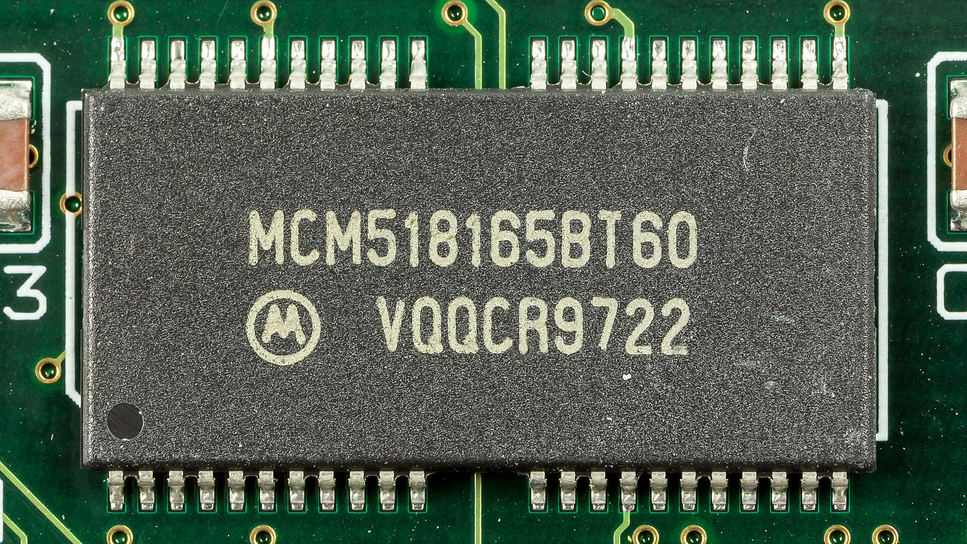
ChangXin Memory Technologies said on Sunday 20 September 2026 that its fifth-generation DRAM platform, which the company calls G5, has entered mass production. Reuters reported from Beijing the same day that CXMT has reduced the spacing of the features that store data to 11.95 nanometres, about 12 billionths of a metre, using quadruple patterning, a technique that repeats several manufacturing steps to draw finer circuit patterns.
The announcement came at the 2026 World Manufacturing Convention in Hefei, the eastern Chinese city where CXMT is based. DRAM is the working memory that phones, computers and servers use to run software. CXMT is China's largest producer of it, and Samsung Electronics, SK Hynix and Micron Technology supply most of the rest of the world.
Our process capability is now on par with the most advanced mass-produced nodes out there in the industry
The number CXMT did not publish
CXMT said the platform can produce at least 50% more gross chip dies per wafer than its fourth-generation platform, measured against an 8-gigabit baseline. Reuters attached the qualifier that matters: gross dies count the chips a wafer could yield before defective units are excluded, not the proportion that passes final testing. Yield decides whether a memory process makes money, and the company gave no figure for it.
The first products on the platform are two 24-gigabit LPDDR5X chips, the low-power memory used in handsets. Both are in mass production and are offered in 496-ball and 245-ball packages for mid-range to high-end smartphones and portable electronics, CXMT told the Global Times on 20 September. Each holds 50% more data than the company's previous equivalent part. CXMT also said it built the platform using computer simulations and joint work with Chinese chip-equipment makers on critical production steps, which is the sentence Washington will read twice.
An $8.6 billion listing behind it
CXMT began trading on Shanghai's STAR Market on 27 July 2026 after selling 6.69 billion shares at 8.66 yuan each, raising 57.92 billion yuan, about $8.6 billion, in what Reuters reported was Asia's largest initial public offering of the year to that point. The shares rose 466% on the first day, Reuters reported, taking CXMT to the top of China's market by valuation. The company said the proceeds would fund memory wafer production and research.
The advance lands while Beijing is pushing to reduce reliance on foreign semiconductor technology and while US export controls, in place since 2022, restrict Chinese access to certain advanced chipmaking equipment and the software that drives it. Quadruple patterning is the route to fine dimensions that does not require the extreme ultraviolet lithography machines those controls keep out. It reaches them by repeating steps, which costs throughput and usually costs yield.
The honest reading is that CXMT has matched its rivals on the dimension it chose to publish and has left the expensive part undisclosed. Against the sceptical case, the company is shipping: the LPDDR5X parts are in production now, not sampling. What nobody outside Hefei can check is the wafer cost per working die, and until a teardown or a customer's own qualification data puts a number on it, 11.95 nanometres remains a vendor measurement of a vendor process.
What happens next?
- Independent teardowns of Chinese handsets carrying the 24-gigabit LPDDR5X parts will test the 11.95-nanometre claim.
- CXMT's first full results as a listed company will show whether its fourth-generation platform was profitable at current memory prices.
- Samsung, SK Hynix and Micron negotiate 2027 mobile DRAM contract prices with a fourth credible supplier now in the room.
- US and allied regulators decide whether multi-patterning at this dimension warrants further restrictions on tools or components.
Related topics
Sources & references
- 01China's CXMT says new memory-chip platform enters mass production — ReutersnewsBeijing, 20 September 2026. Source of the 11.95-nanometre figure, the quadruple patterning description, the gross-dies caveat and the Luo Xiaodong quote.
- 02Chinese chipmaker CXMT's 5th-generation memory-chip platform enters mass production, marking new breakthrough in process scaling — Global TimescompanyCXMT's own statement to the outlet, 20 September 2026. Source of the 496-ball and 245-ball package detail and the 45:1 capacitor aspect ratio.
- 03Chinese chipmaker CXMT to list in Shanghai on July 27 after Asia's biggest IPO this year — Reutersnews23 July 2026. Source of the 6.69 billion shares at 8.66 yuan and the 57.92 billion yuan total.
- 04Chipmaker CXMT vaults to top of China's valuation with 466% surge in Shanghai debut — Reutersnews27 July 2026. Source of the 466% first-day rise.
More from Technology
SK Hynix Weighs Making Memory Chips at Intel's Ohio Site
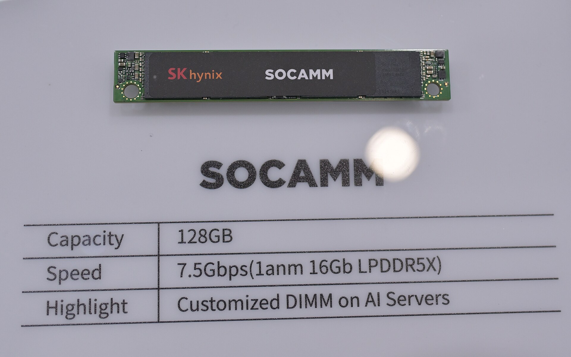
SK Hynix is in talks with Intel about manufacturing memory chips in the United States for the first time, three people familiar with the discussions told Reuters on 16 September 2026. One option is leasing part of Intel's Ohio complex, whose two plants have slipped to 2030 and 2031; another is a venture with Intel and cloud firms seeking memory supply. Any deal involving HBM or DRAM could face review under South Korea's Industrial Technology Protection Act.
The Chip Industry Agrees to Change a Forty-Year-Old Standard
High-NA EUV's optics halve the exposure field, forcing large AI dies to be stitched from two exposures at a heavy throughput cost. On 8 September 2026 the leading-edge industry aligned on a move to 12-inch masks, with TSMC targeting High-NA in high-volume manufacturing from 2030 and Samsung planning High-NA for DRAM by 2028.
Amazon Takes a Stake in Its Next Chip Supplier
Qualcomm announced a multi-generation collaboration with Amazon on custom AI inference silicon and 1.6T optical connectivity on 8 September 2026. An SEC filing shows Amazon received a warrant for up to 25 million Qualcomm shares at $161.26, vesting in tranches tied to commercial arrangements and purchases up to a $60 billion cap.
The Inference Economy
A data story on why inference is overtaking training as the dominant compute and cost story, and what it means for chips, data centres and pricing.